
Jane Street put out a challenge to reverse engineer an ASIC from it's GDS file. This was quite the fun reverse engineering problem, going from logic gates to understanding a full chip. I worked with my good friend Armaan Gomes on this project. Here's how we did it, and the solution to the puzzle.
Oh and by the way, it's my birthday! \(^o^)/
Going from GDS to Spice
A GDS file is essentially a 3D model a designer would send to a fab to fabricate the ASIC. In order to make it easier to analyze the circuit we converted it to a representation called Spice. Armaan analyzed the GDS using the IIC-OSIC-TOOLS docker image and Magic. Then, he used ext2spice and the sky130 pdk to lift the spice netlist out of Magic. Then, he used Claude to help make a short python script to convert the spice into Verilog using the sky130 primitives. The resulting Spice looks like this:
[...]

Xsky130_fd_sc_hd__and2_2_4 sky130_fd_sc_hd__or4_2_2/A sky130_fd_sc_hd__and4_2_1/B
+ sky130_fd_sc_hd__or4_2_2/B VPWR VGND VPWR VGND sky130_fd_sc_hd__and2_2
Xsky130_fd_sc_hd__dfrtp_2_7 sky130_fd_sc_hd__inv_2_2/A rst_n sky130_fd_sc_hd__o21a_2_9/X
+ sky130_fd_sc_hd__clkbuf_8_1/X VGND VPWR VPWR VGND sky130_fd_sc_hd__dfrtp_2

[...]
And the converted Verilog looks like this:
[...]

  assign _0038_ = \sky130_fd_sc_hd__a21oi_2_13.B1  ^ _0796_;
  assign \sky130_fd_sc_hd__dfrtp_2_43.D  = _0708_ & _0038_;

[...]
The gates of the ASIC are described in the Spice with this format: [Gate Name] [Wire A] [Wire B] ... [Wire X] [Gate Type]. The + just indicates that the line break should be ignored. For example, this code snippet above describes two gates. The first gate is named Xsky130_fd_sc_hd__and2_2_4 and is a sky130_fd_sc_hd__dfrtp_2 which is a sky130 flip flop. One thing to note is that it isn't obvious which wires are inputs and outputs of this gate. While there is a pattern kind of, I chose instead to hardcode the input and output port names of every gate type used in the ASIC.
Spice to Logic
After we had generated the Spice, the next step was to start writing code to parse the circuit and transform it to representations that are nicer to work with. I wrote a Deno script that essentially took the Spice, converted it to an undirected graph, then traversed this graph from the circuit ports to generate a directed graph of gates connected to each other. The important thing here is that we went from Spice to a nice graph of logic gates with their input and output connections.
The script also applied three passes to the circuit graph:
- Remove gates not connected to success output port
- Remove clock buffer gates
- Infer registers from
flip flop -> muxpattern
These passes cleaned up the graph a little bit which would help later down the line. Not every "register" fit the pattern of flip flop -> mux. Most of the instances of flip flops acted more like a buffer that buffered some value rather than as a register with a write enable. Because of this, I elected to leave the other flip flops be.
To help visualize what the circuit looked like, I wrote a small webapp that used the sigma library to visualize the graph.
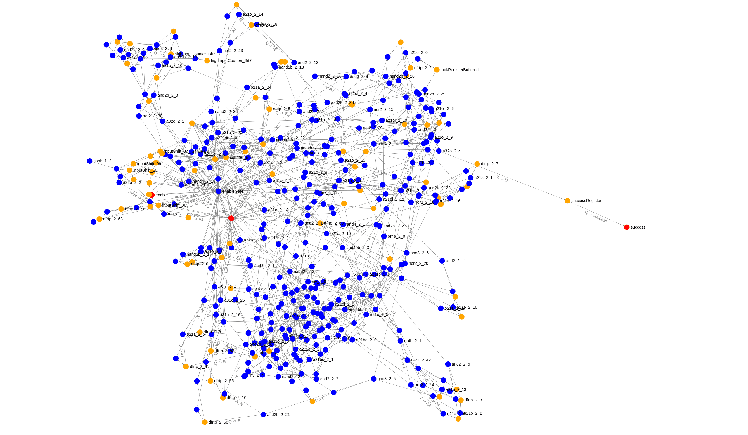
This visualization was nice because it helped ground my picture of the circuit to something visual instead of just an abstract collection of gates. However, in the end this visualizer didn't help out much with reversing the logic in the circuit. It was just too difficult to manipulate and too confusing to read.
Within this graph, there is a huge variety of gate types. Here's the list of every type I needed to handle:
- sky130_fd_sc_hd__mux2_1
- sky130_fd_sc_hd__and2_2
- sky130_fd_sc_hd__and2b_2
- sky130_fd_sc_hd__and3_2
- sky130_fd_sc_hd__and3b_2
- sky130_fd_sc_hd__and4_2
- sky130_fd_sc_hd__and4b_2
- sky130_fd_sc_hd__and4bb_2
- sky130_fd_sc_hd__or2_2
- sky130_fd_sc_hd__or3_2
- sky130_fd_sc_hd__or3b_2
- sky130_fd_sc_hd__or4_2
- sky130_fd_sc_hd__or4b_2
- sky130_fd_sc_hd__or4bb_2
- sky130_fd_sc_hd__xor2_2
- sky130_fd_sc_hd__nand2_2
- sky130_fd_sc_hd__nand2b_2
- sky130_fd_sc_hd__nand3_2
- sky130_fd_sc_hd__nand3b_2
- sky130_fd_sc_hd__nand4_2
- sky130_fd_sc_hd__nor2_2
- sky130_fd_sc_hd__nor3_2
- sky130_fd_sc_hd__nor3b_2
- sky130_fd_sc_hd__nor4_2
- sky130_fd_sc_hd__nor4b_2
- sky130_fd_sc_hd__xnor2_2
- sky130_fd_sc_hd__inv_2
- sky130_fd_sc_hd__a21o_2
- sky130_fd_sc_hd__a21bo_2
- sky130_fd_sc_hd__a211o_2
- sky130_fd_sc_hd__a22o_2
- sky130_fd_sc_hd__a31o_2
- sky130_fd_sc_hd__a32o_2
- sky130_fd_sc_hd__a311o_2
- sky130_fd_sc_hd__a221o_2
- sky130_fd_sc_hd__o2bb2a_2
- sky130_fd_sc_hd__o21a_2
- sky130_fd_sc_hd__o21ba_2
- sky130_fd_sc_hd__o22a_2
- sky130_fd_sc_hd__o211a_2
- sky130_fd_sc_hd__o311a_2
- sky130_fd_sc_hd__o31a_2
- sky130_fd_sc_hd__o221a_2
- sky130_fd_sc_hd__o32a_2
- sky130_fd_sc_hd__a21oi_2
- sky130_fd_sc_hd__a21boi_2
- sky130_fd_sc_hd__a211oi_2
- sky130_fd_sc_hd__a31oi_2
- sky130_fd_sc_hd__a22oi_2
- sky130_fd_sc_hd__a221oi_2
- sky130_fd_sc_hd__a41oi_2
- sky130_fd_sc_hd__a2111oi_2
- sky130_fd_sc_hd__o21ai_2
- sky130_fd_sc_hd__o21bai_2
- sky130_fd_sc_hd__o211ai_2
- sky130_fd_sc_hd__o22ai_2
- sky130_fd_sc_hd__o31ai_2
- sky130_fd_sc_hd__o32ai_2
- sky130_fd_sc_hd__dfrtp_2
- sky130_fd_sc_hd__dfstp_2
- sky130_fd_sc_hd__dfxtp_2
- sky130_fd_sc_hd__decap_3
- sky130_fd_sc_hd__diode_2
- sky130_fd_sc_hd__clkbuf_16
- sky130_fd_sc_hd__clkbuf_8
- sky130_fd_sc_hd__clkbuf_4
- sky130_fd_sc_hd__buf_2
- sky130_fd_sc_hd__conb_1
Yeah, it wasn't very fun to write the code to manage all of these gates by hand.
Logic to JavaScript?
I think a huge part of reverse engineering is being able to manipulate and annotate the obfuscated code / logic you're trying to understand. Being able to move things around, label things, and simplify things helps immensely with understanding. This is why the graph visualization ended up being insufficient. So, I wrote a converter that turned the logical circuit graph into a sort of pseudo JavaScript. At first, it looked like this:
const nand2_2_23 = nand2_2({B: enableGate.X, A: enableLockCondition1.X})
const a31o_2_8 = a31o_2({A2: enableGate.X, B1: dfrtp_2_15.Q, A3: dfrtp_2_16.Q, A1: enableLockCondition1.X})
const and4_2_2 = and4_2({B: enableGate.X, C: dfrtp_2_15.Q, D: dfrtp_2_16.Q, A: enableLockCondition1.X})
const inv_2_5 = inv_2({A: and4_2_2.X})
const o211a_2_7 = o211a_2({A2: nand2_2_23.Y, B1: a31o_2_8.X, A1: nand3b_2_0.Y, C1: inv_2_5.Y})
dfrtp_2_15.next = dfrtp_2.eval({RESET_B: io.rst_n, CLK: io.clk, D: o211a_2_7.X})
const xor2_2_9 = xor2_2({A: dfrtp_2_17.Q, B: and4_2_2.X})
dfrtp_2_17.next = dfrtp_2.eval({RESET_B: io.rst_n, CLK: io.clk, D: xor2_2_9.X})
const a21o_2_9 = a21o_2({A1: dfrtp_2_17.Q, B1: dfrtp_2_18.Q, A2: and4_2_2.X})
const nand3_2_0 = nand3_2({A: dfrtp_2_17.Q, B: dfrtp_2_18.Q, C: and4_2_2.X})
const o311a_2_1 = o311a_2({A1: dfrtp_2_16.Q, A3: nand2_2_23.Y, A2: nand3b_2_0.Y, C1: a21o_2_9.X, B1: nand3_2_0.Y})
I could rename gates, move things around, and generally edit everything like you could normally with a text file. This was a start, but as you might imagine, reading the logic was still near impossible. Everything's jumping around everywhere and linking to each other. I needed to simplify the code even more. So, I extended the code to convert every gate to JavaScript boolean logic, which looked like this:
const counter_Bit0 = new Register(!(counterIs11 || (counter_Bit0 === enableGate)), rst_n) // counter_Bit0
const and3_2_14 = (counter_Bit1 && counter_Bit0 && enableGate) // and3_2_14
const counter_Bit1 = new Register(!((enableGate && counterIs11) || !((counter_Bit0 && enableGate) || counter_Bit1) || and3_2_14), rst_n) // counter_Bit1
const counter_Bit2 = new Register((counter_Bit2 !== and3_2_14), rst_n) // counter_Bit2
const counter_Bit3 = new Register(!((enableGate && counterIs11) || ((counter_Bit1 && counter_Bit0 && counter_Bit2 && enableGate) && counter_Bit3) || !((counter_Bit1 && counter_Bit0 && counter_Bit2 && enableGate) || counter_Bit3)), rst_n) // counter_Bit3
const counterIs11 = (!counter_Bit0 && !counter_Bit2 && counter_Bit3 && counter_Bit1) // counterIs11
Not exactly easy to read, but much more familiar and understandable. Another nice thing about the JS was that it tended to group related registers very close to each other. This helped a ton.
With just this generated JavaScript, I was able to start understanding what actually was going on in the circuit. The first bit of logic I was able to crack was two counters. Originally I thought there was one large 8 bit counter, but it was actually two smaller 4 bit counters. By working out the boolean logic on paper, I figured out that both counters counted to 11. When the first counter reached 11 it would increment the second counter by 1 before resetting. This in combination with the circuit taking only 1 bit of input and noticing that we get output on the 121st cycle, we were able to deduce that there was likely some sort of 11x11 grid we had to solve.
One important thing we did, was after I discovered the function of some logic by analyzing the pseudo JavaScript, I would ask Armaan to run a test using the simulation to verify that our understanding was correct.
Now wary of counters, I found another 8 bit counter that counted how many true inputs were supplied and success was conditioned on this counter being exactly 22.
Discovering the Column Constraint
My main methodology was to try to start at the registers and understand the logic providing their next value. This helped a ton because every register ended up indicating something rather concrete about the puzzle. For example, the registers I reversed earlier stored the current cell location on the 11x11 grid or the fact that we needed exactly 22 true inputs.
I decided to tackle another group of registers that seemed to be the next most manageable bit of logic. Once again I played around with the logic on paper and in the text file. The first important thing I noticed was that the registers seemed to come in pairs. The success signal logic grouped them like this:
const successRegister = !failRegister1 && !failRegister2 && highInputIs22 &&
  !lockRegisterBuffered && lockRegister &&
  !dfrtp_2_6 && dfrtp_2_11 &&
  dfrtp_2_13 && !dfrtp_2_7 &&
  !dfrtp_2_53 && dfrtp_2_10 &&
  !dfrtp_2_5 && dfrtp_2_12 &&
  dfrtp_2_2 && !dfrtp_2_1 &&
  !dfrtp_2_0 && dfrtp_2_14 &&
  !dfrtp_2_8 && dfrtp_2_4 &&
  dfrtp_2_3 && !dfrtp_2_9 &&
  !dfrtp_2_56 && dfrtp_2_59 &&
  dfrtp_2_52 && !dfrtp_2_54 &&
  !dfrtp_2_55 && dfrtp_2_58 &&
  !dfrtp_2_80 && dfrtp_2_66 &&
  dfrtp_2_79 && !dfrtp_2_65 &&
  !dfrtp_2_75 && dfrtp_2_67 &&
  !dfrtp_2_78 && dfrtp_2_64 &&
  dfrtp_2_61 && !dfrtp_2_76 &&
  !dfrtp_2_60 && dfrtp_2_57 &&
  !dfrtp_2_71 && dfrtp_2_63 &&
  dfrtp_2_77 && !dfrtp_2_62 &&
  !dfrtp_2_74 && dfrtp_2_70 &&
  io8Twice && !io8NotTwice &&
  !dfrtp_2_73 && dfrtp_2_68;
And, the registers shared similar negated logic in pairs:
const dfrtp_2_68 = new Register(!(dfrtp_2_68 && !(io && dfrtp_2_73 && counterIs10)), rst_n) // dfrtp_2_68
const dfrtp_2_73 = new Register(((dfrtp_2_68 || !(io && dfrtp_2_73 && counterIs10)) && ((io && counterIs10) || dfrtp_2_73)), rst_n) // dfrtp_2_73
I also noticed there happened to be exactly 22 registers that followed this pattern closely. This made me suspicious it might be something to do with the rows or columns of the grid I predicted earlier.
By analyzing the logic on paper, I figured out that these registers each corresponded to one column and tracked that exactly two true values were placed on that column. If any less or more than two true values existed on a single column of the 11x11 grid, then success would not be able to pass. This essentially confirmed to me that we were working with some kind of grid. On top of the column constraint, the registers would fail if any two stars were directly adjacent to another, diagonal or orthogonal.
As a quick guess I asked Armaan to try and see if the circuit would pass success if we passed in a grid where there were exactly 22 true values, every row and column contained exactly two true cells, and no adjacent true cells. Unfortunately this didn't work, we still had some ways to go.
Brute Force
Along with some miscellaneous additional logic, there was one last major block of registers we hadn't figured out yet. The combination logic feeding into these registers was much larger than the other ones. It seemed rather infeasible to figure out the logic by hand. In an attempt to make it more understandable I started working on a circuit graph pass that would convert all of the complex sky130 gates into just a few base gates:
- or
- and
- not
- xor
The idea was that once everything had been converted to base gates, it might be easier to infer half adders and other math operations.
After implementing the new circuit graph pass, I tried taking a look at the generated pseudo JavaScript. Because of the conversion to simpler operations, the JavaScript generator added a lot more parenthesis which actually heavily impacted the performance of my VSCode when the file was open.
However, while analyzing this new massive file, I realized that the massive logic was actually only a function of the input signal I and the cell locations counters. Not only that, they seemed to also resemble the same paired logic that ensured exactly 2 trues were placed in each column. With these insights, I wrote a Verilator simulation to brute force all possible 121 locations for each of the registers to discover which locations triggered the logic. After recording which locations of the grid triggered for each register, and color coding the cell based on the register, I got this image:

We can clearly see JSC drawn out by the regions, likely standing for Jane Street Capital! At this point I knew we were close and on the right track.
After a tiny bit more work figuring out a final three registers, which turned out to enforce exactly two trues per row, I asked Armaan to help me come up with a solution with the following constraints:
- Each row must have exactly 2 true cells
- Each column must have exactly 2 true cells
- Each colored group in the image must have exactly 2 true cells
- No adjacent true cells
Armaan came up with this solution:
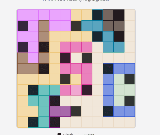
Which corresponds to the input string:
00000001010
10000100000
00000001010
10100000000
00001010000
00100000100
00001000001
01000010000
00010000001
00000100100
01010000000
Piping this input into the circuit in simulation not only triggers success but outputs (* TWO STARS *)! One other easter egg we found was that entering all trues outputs BIG BANG. Also, I bet the ASIC was programmed in HardCaml. (* *) is the comment syntax in OCaml.
Conclusion
And with that we solved the ASIC. I think one of the most fun aspects of reverse engineering is that every time you figure out some new part of the program, it feels like a super awesome insight you discovered. There were certainly a number of those moments as we worked through everything.
On top of this, all of the reverse engineering work was done without the use of LLMs. Every single thing we discovered was purely human understanding about an obfuscated system. Claude was used minimally to help with debugging some of the tooling, but we never gave the SPICE or any of the pseudo JS generated from it to an LLM.
Thank you to Armaan for helping me on this project, and thank YOU for being curious enough to read this blog! Also thanks to the people at Jane Street for creating this puzzle.
If you thought this was interesting, you might be interested in reading about how we ran DOOM at 60fps on our RISC-V CPU design and going viral.