
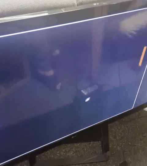
This is a RISC-V processor from scratch with no hardware design experience. Just recently, we achieved compiling a pong program written in C to the processor and displaying interactive video on a display through VGA. If you're interested in how CPUs work, hardware design, or just want to see a processor designed from scratch, this blog is for you.
What Can the CPU Do
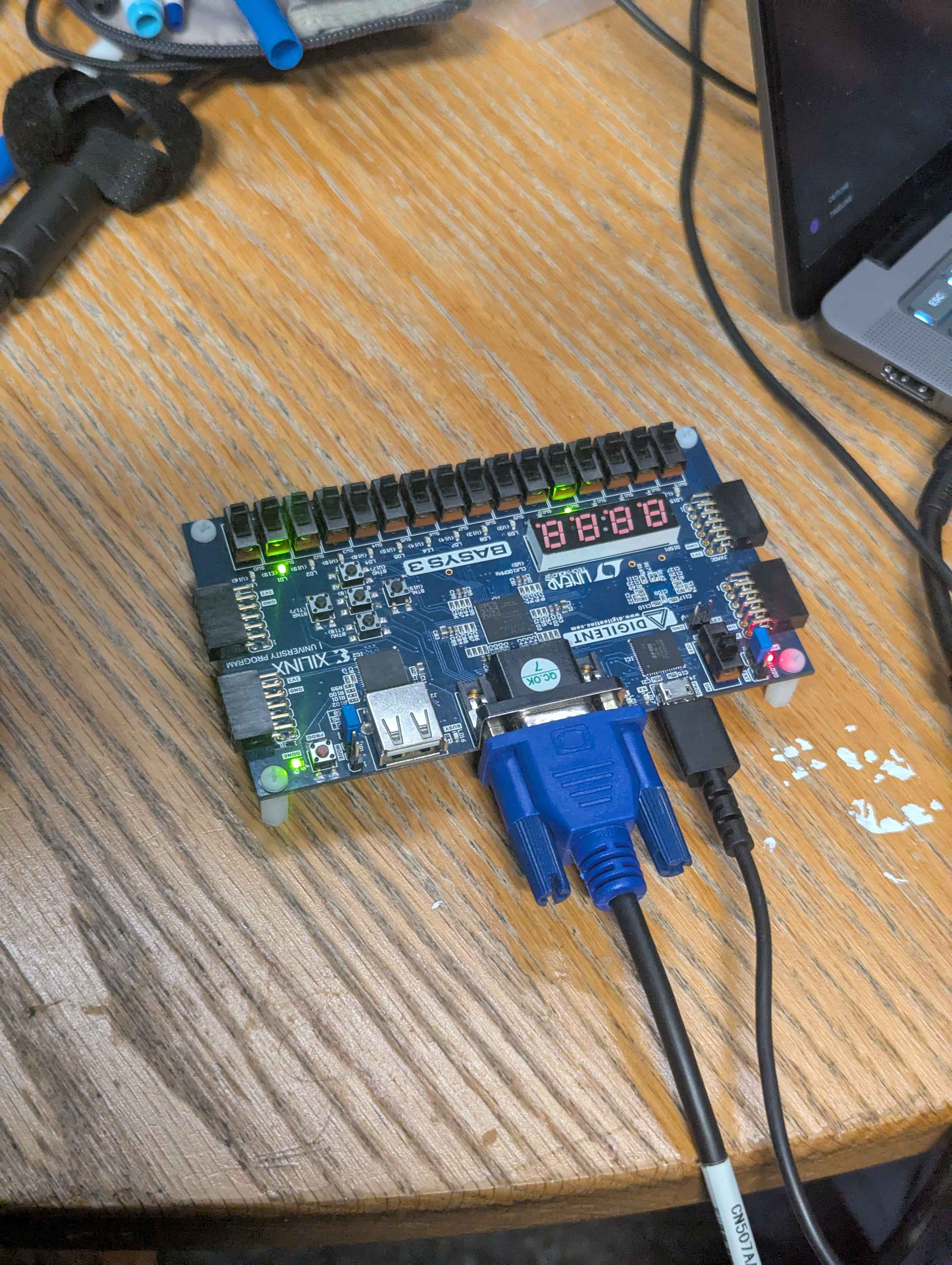
The CPU conforms to the RISC-V unprivileged integer instruction specification. This means it can execute any programs compiled for this architecture. The CPU has one core and has part of it's memory address spaced mapped to a 320x240 8-bit color framebuffer for displaying video on a screen, as well as a space in adress mapped for reading input from buttons directly on the board. The clock runs at 25 Mhz and can execute one instruction per every 2 clock cycles. (Except for memory instructions, which take three clock cycles). This is definitely not the fastest we can go. I can think of one easy optimization that would double our speed right now, but that's for future me. The CPU design is also being run on an FPGA board. We are planning on doing a real tapeout of the CPU to get it on real silicon, but we want to improve the processor's performance before we spend the money to do a tapeout.
How It Works
The four main important components of the processor are the:
- Memory Controller
- Decoder
- Instruction Logic
- VGA Controller
Memory
On our FPGA we have to be careful about how we configure our memory. We only have a limited number of read-write ports into BRAM, which is where we are storing our program and all of the program's memory. The memory controller's job is to help manage our memory and redirect any special memory requests to the write components. On the current design of the processor we define about 4KB of memory with 32 bit wide read-write ports. The memory is addresseble for every 32 bits so we often need to use both read-write ports to handle memory reads and writes that fall across these memory boundries. The size of our memory is kind of just an arbitrary number and isn't capped at 4kB, that's just what we had defined when we were running pong.
The memory controller also has special address ranges designated for special behaviours. Any address from 0x4000 to 0x4AFFFFFF would instead write to a framebuffer for the VGA display. Any read at 0x4B000000 would return the state of 4 buttons on the FPGA board. This way, programs could easily interface with the extra component on the board by simply reading and writing to memory.
Decoder
When we fetch an instruction from memory, we send it through our Decoder module. This helps decode any immediate values in the instructions and helps simplify the instruction logic. Hilariously, like other parts of this CPU, the Decoder is essentially just one giant switch statement that routes bits from the encoded instruction to the right places.
This is a snippet from our Decoder.scala file:
switch(opcode) {
    is(0b0110111.U) { format := InstructionFormat.U; } // lui
    is(0b0010111.U) { format := InstructionFormat.U; } // auipc
    is(0b0010011.U) { format := InstructionFormat.I; } // addi, slti, sltiu, xori, ori, andi, slli, srli, srai
}

switch(format){
    is(InstructionFormat.R) {
        io.operation := io.instruction(31,25) ## io.instruction(14,12) ## io.instruction(6,0);
    }
    is(InstructionFormat.I) {
        io.operation := io.instruction(14,12) ## io.instruction(6,0);
        io.immediate := Fill(21, io.instruction(31,31)) ## io.instruction(30,20);
    }
    is(InstructionFormat.S) {
        io.operation := io.instruction(14,12) ## io.instruction(6,0);
        io.immediate := Fill(21, io.instruction(31,31)) ## io.instruction(31,25) ## io.instruction(11,7);
    }
}
Instruction Logic
The instruction logic is also a giant switch statement, except this time the switch statement affects registers and memory. For simplicity, until we implement out of order execution, the CPU has a simple stage system. During stage 0, the instruction is loaded from memory. In stage 1, most instructions execute. Some instructions that deal with memory also have a stage 2, where they do some additional work since reading from BRAM takes a clock cycle.
when(stage === 1.U) {
    switch(decoder.io.operation) {
        // LB
        is("b000_0000011".U) {}

        // LH
        is("b001_0000011".U) {}

        // LW
        is("b010_0000011".U) {}

        // LBU
        is("b100_0000011".U) {}
    }
}
VGA Controller
To render video to a screen, the CPU also contains a VGA controller. The VGA controller defined a chunk of 320x240 8-bit memory for the framebuffer. The VGA controller would then render this framebuffer onto any display connected to the VGA input on the FPGA board. The resolution that the VGA controller emits is actually 640x480, but because of the limited memory on the FPGA, we chose to make the framebuffer at half resolution.
How We Made It
This project is actually a collaboration between some of the members of MIT OpenCompute. The vast majority of the code of the current design is written by me. Armaan Gomes helped a ton with his HDL experience and getting the design actually running on an FPGA. Ryan Tang helped out with some initial code setting up the project.
The CPU design is written in a hardware description framework called Chisel. Chisel allows us to write scala code that compiles to Verilog for simulation and synthesis.
During the inital work on the processor and up until these last few days, where we syntehsized the design onto the FPGA, I used a lot of Verilator simulations to inspect the processor to make sure it at least worked logically. Honestly, I'm surprised at how well the same design transferred over to the real FPGA hardware. We effectively only had to modify our memory controller to fit the constrained read-write ports on the FPGA.
As I said at the beginning, I didn't have experience with hardware design. I have a lot of experience programming and some experience reverse engineering, so I have looked at how x86 instructions are encoded in memory and also how to write x86 assembly. Of course, I have also read parts of the RISC-V specifications to help implement the proper instruction formats. From there, this entire CPU design is kind of just an extrapolation of this. I guess it just goes to show how much you can figure out just by imagining how something might work.
What's Next?
There are a number of ways we can upgrade the design. I want to look into out of order execution to speed up processing. I also want to implement more RISC-V extensions. Eventually, we’ll hopefully even tape out the design and have the processor design on real silicon!
Thanks for reading, and if you have any questions, contact me!